UBM (OPM: Over Pad Metal, FSM: Front Side Metal and Electroless plating) Service
Flip chip bonding is increasingly taking over conventional wire bonding for bonding of microchips, as semiconductor packaging technology advances toward smaller sizes and higher density. Under Bump Metallurgy (UBM) formation to bond metal pads to solder is considered to be essential in flip chip bonding. Our UBM process makes use of electroless plating technology, offering advantages such as lower cost, faster delivery, and smaller size, as well as consideration for the environment.
| Product Category | Thin film materials |
|---|---|
| Main Products | Electroless UBM plating service |
| Primary Applications | Bonding of microchips to the substrate |
What is "UBM"?
"UBM" stands for Under Bump Metallurgy (also described as Under Bump Metal or Under Barrier Metal) and is applied to provide solderability to electrodes of semiconductor wafers. UBM is formed by plating wafers or other methods (then UBM is sometimes called as "top metal plating"). Our UBM formation service has a characteristic of wafer plating (semiconductor plating) processing by electroless (E-less or Eless) plating. Specifically, electroless nickel gold plating layer (ENIG) or electroless nickel palladium gold plating layer (ENEPIG) is formed on wafer electrodes as UBM layer. UBM layer is also commonly applied for more robust base of wire bonding. UBM is also called as "OPM" (Over Pad Metal) and "FSM" (Front Side Metal) in this application.
Specifications of our UBM Plating Service
Specifications and properties
| (Specification) | *Trial production | |
|---|---|---|
| Wafer | Si, GaAs (other materials also supported) | As on the left + SiC |
| Wafer size | 50-300mmφ (2"-12") | |
| Wafer thickness | 150 µm or larger (consult with us about sizes smaller than 150 µm) | Min.80um (6"φ) |
| Pad material | Pure Al, AlSi, AlCu, AlSiCu, Cu, Au | |
| Pad shape | Square, round, other | Min. aperture of 4 µm square |
| Applications | Logic, memory, power transistors, MEMS, etc. | |
| UBM | Electroless Ni/Au, electroless Ni/Pd/Au (Pb-free, CN-free bath used) |
| Ni (material) | Ni (P 5-10%) |
|---|---|
| Ni thickness | 1 to 5 µm: There are space constraints between pads |
| Pd thickness | 0.05-0.2µm |
| Au thickness | 0.02-0.05µm (Ni/Pd/Au) 0.05-0.10µm (Ni/Au) |
| Thickness uniformity | ±10% or less (200mmφ) |
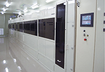
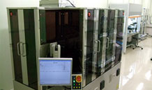
UBM plating lines
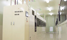
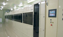
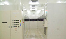
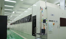
- Features of plating line
- Clean room: Class 1,000
- Manufacturing on program-controlled automated lines
- Service provided in two locations, in Japan and Taiwan
Features of our Electroless UBM Plating Service
Features
- Potential difference reduced with self-developed process
- Provides a reliable quality control system using our own extensive analysis and evaluation equipment
- Support for wafer sizes of up to 12 inches
Our in-house evaluation and inspection equipment
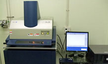
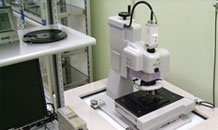
Our in-house analytical equipments
| Surface morphology investigation | FIB-SEM, FE-SEM, SPM |
|---|---|
| Surface element analysis | FE-EPMA, FE-AES, XPS |
| Surface functional group analysis | Raman, FT-IR, UV |
| Metal and crystal structure analysis | XRD |
⇒Surface structure and elemental analysis equipment, which were accumulated for R&D of semiconductor related products.
Features of Our Process Based on our self-developed process
Suppressing thickness variation caused in potential difference due to differences of IC pad type and size
Our electroless UBM plating process provides uniform quality of UBM, even for pads with differences in electrical potential or size with proprietary additives and plating techniques.
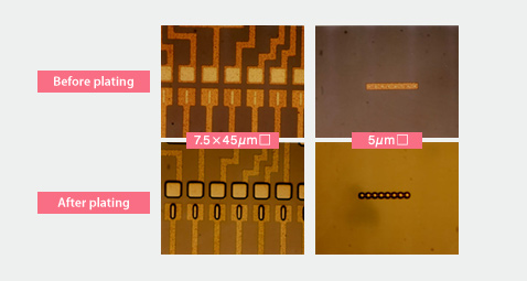
Uniform plating on small pads.
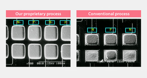
Less thickness variation on pads with different potential.
Strengthening solder joint by suppressing pitting corrosion in electroless Au plating
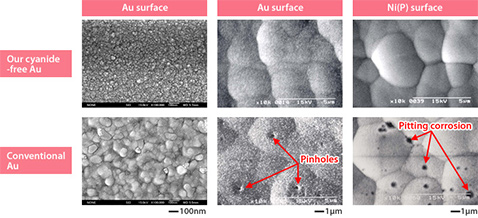
Our electroless Au plating bath is cyanide-free, and we have succeeded in practically eliminating pitting corrosion in Au plating layers with special additives. Stronger solder joint is achieved as a result. In addition, we have further enhanced solder joint strength by analyzing plating solutions and plated films, and feeding back the results into plating solution development.
High reliability in wire bonding strength
The advantages of our electroless plating are seen not only in flip chip bonding, but also in use as OPM (over pad metal) for wire bonding.
Compliant with environmental regulations such as Pb-free
Our electroless UBM plating bath is environmentally considerate process, which contains no cyanide or other toxic materials, and no lead or other materials restricted under the RoHS Directive.
Inquiries accepted 24 hours a day