Compound Semiconductors and Crystal Materials
Compound Semiconductor Substrates (InP, CdZnTe, CdTe)
JX Metals's Products with their consistently high quality are winning customer acclaim and confidence. We manufacture InP for III-V compound semiconductors, and Cd(Zn)Te for II-VI compound semiconductors. We supply products meeting the latest demand and product requirements.
| Product Category | Thin Film Materials |
|---|---|
| Main Products | InP (indium phosphide) and CdZnTe (CdTe) (cadmium telluride) |
| Primary Applications | Light emitting elements, light receiving elements, high-speed electronic devices, infrared detectors, radiation detectors, etc. |
| Catalog | [Product Catalog: English-language edition] InP, CdTe |
Lineup
| Size | Orientation | Dopant | |
|---|---|---|---|
| InP | 2inch 3inch 4inch |
(100) | S, Sn, Zn, Fe, None |
| Size(mm) | Orientation | Dopant | |
|---|---|---|---|
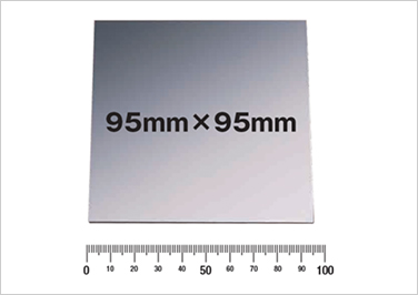
| CdZnTe | 10×10- 95×95 |
(111),(211),(100) | Zn, None |
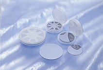
InP Substrates
Application Examples

Mobile Base Stations

Data Centers
Optical Modules
(Light Emitting Elements, Light Receiving Elements)

Solar Power
Features of JX Metals's InP Substrates
- We have long been providing InP substrates as essential materials for light emitting and receiving elements in optical communications.
- With the world’s highest quality, they continue to boast the top share globally.
- For improved device quality, we provide wafers with high processing precision.
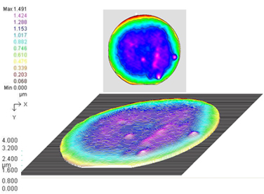
*Total Thickness Variation
Proposals for new InP applications
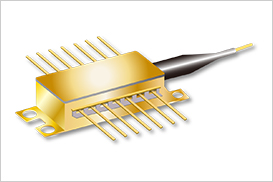
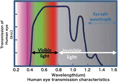
High-performance collision prevention sensor made feasible

Laser radar at eye-safe wavelength made feasible
CdZnTe Substrates
Application Examples

Radiation Sensors for Medical and Analysis Use

Infrared Sensors for Space and Environmental Use

Solar Power
Features of JX Metals's CdZnTe Substrates
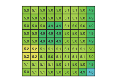
- Large-diameter CdZnTe single crystals of the world’s highest quality are achieved using our proprietary crystal growing technology.
- CdZnTe can detect radiation with higher precision than other materials, for stable X-ray detection.
- Our CdZnTe substrates with uniform Zn concentration enable customers to produce larger infrared sensors.
Contact Information
From the Web
Inquiries accepted 24 hours a day
By telephone
- Department name
- Compound Semiconductor Department, Thin Film Materials Division
Calls accepted from 9:00 a.m. to 5:50 p.m. JST (except weekends and holidays)