News Release
FY2023
June 26, 2023
Full-scale Marketing of Mg2Si Single Crystal Material for Semiconductor Devices Jointly Developed with Ibaraki University
-Promoting Efforts for Social Implementation of Next-generation Materials Contributing to Advanced Optical Sensing-
JX Nippon Mining & Metals Corporation (President: Hayashi Yoichi; "the Company") is conducting joint research with the College of Engineering, Ibaraki University on magnesium silicide (Mg2Si) single crystals, a material for new semiconductor devices that will contribute to advanced optical sensing technologies. The Company has now decided to launch full-scale marketing of this product with a view to social implementation. It will raise awareness of the product by exhibiting at trade fairs,* communicate with manufacturers that develop and produce semiconductor devices such as infrared detectors, explore promising applications, and prepare a product business plan.
As digitalization advances in societies on a global scale, optical sensing technology is developing at a remarkable pace in a wide array of fields including automated driving, medical treatment, disaster prevention and security, and food inspection. Such optical sensing technologies use semiconductor substrates to convert a broad range of wavelengths--including infrared as well as visible light--into electrical signals. Various technology development efforts are underway aimed at future utilization of optical sensing devices in diverse fields, but pairing cost performance with detection performance across a broad wavelength range remains a challenge to widespread use. The Mg2Si single crystals that Professor Udono Haruhiko of the College of Engineering, Ibaraki University is researching and developing can detect light across a broad wavelength range from visible light to short-wave infrared. Since the crystals use universally available materials, they offer both detection performance and cost performance, and thus uses can be anticipated in not only industrial applications, but also consumer products.
The Company has been conducting joint research on this product with the College of Engineering, Ibaraki University since 2019. In the aim of expanding its crystal materials business, as set out in the recently released our group Medium-Term Management Plan for FY2023-25, it has now decided to step up commercialization of the product and gather information that will contribute to commercialization decisions through communication with potential customers. The Company's immediate objective is to ship samples halfway through the current Medium-Term Management Plan period. In parallel with these efforts, the Company and Ibaraki University will continue R&D in areas such as increasing ingot size, which is essential to swift social implementation of the product.
Our group will continue to proactively engage in product development through co-creation with its partners, unite in steady implementation of its growth strategy, and contribute to innovation and social development as a global leader in advanced materials.
*This product will be exhibited in the Company's display at LASER World of PHOTONICS 2023, to be held on June 27-30 in Munich, Germany. The event marks the start of product display, and active exhibition of the product is planned for the future. Please click here for exhibition information details.
For reference:
<Magnesium silicide (Mg2Si)>
- Mg2Si is a semiconductor material that can detect light across a broad wavelength range from visible light (VIS) to near infrared (NIR) and short-wave infrared (SWIR) and is expected to be utilized for various types of optical sensors. Since it also exhibits high performance as a thermoelectric material, it is also attracting attention as a next-generation thermoelectric conversion material.
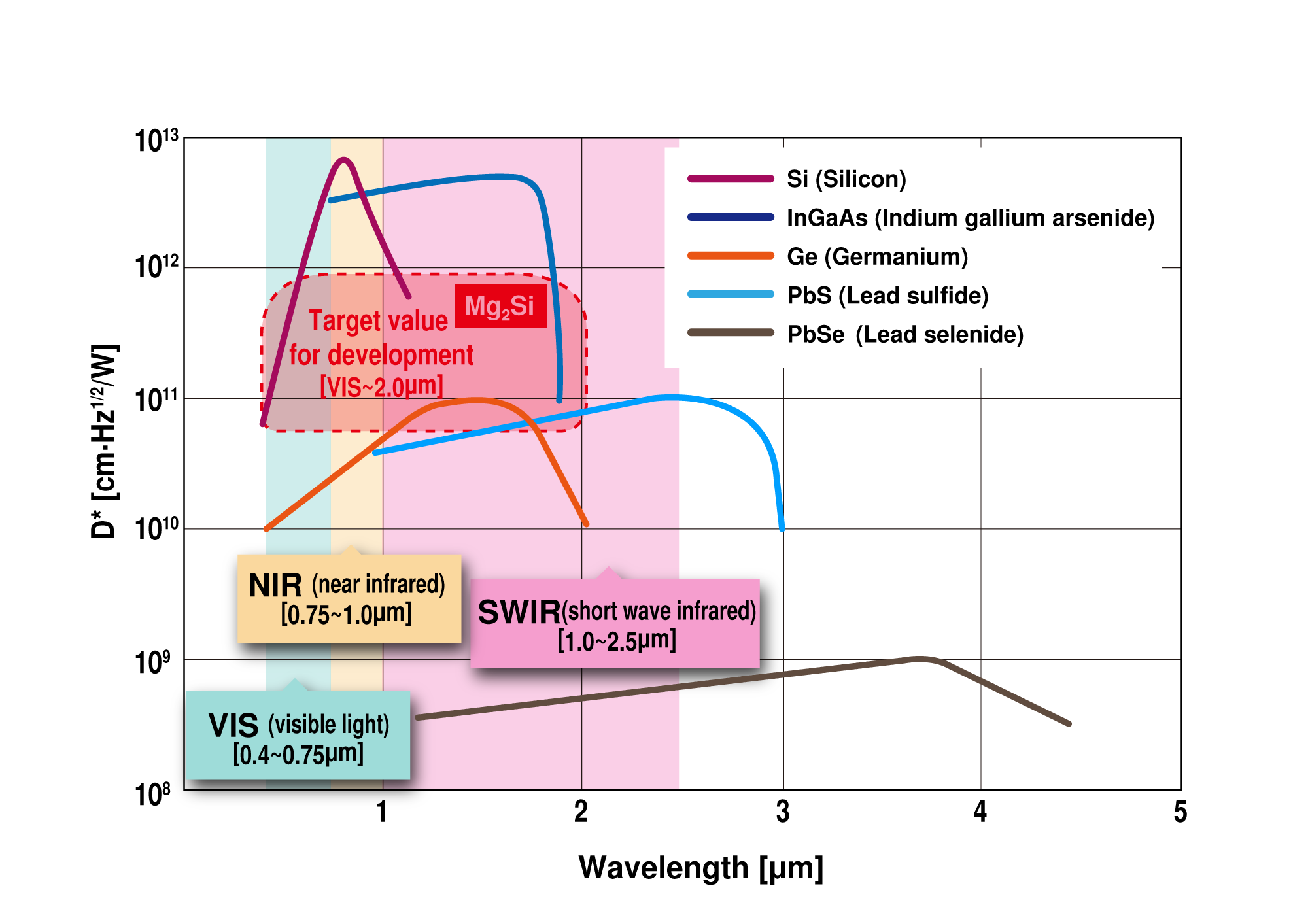
Figure 1: Detection Wavelength Range and Sensitivity Coefficient D* (room temperature) of Various Crystal Materials
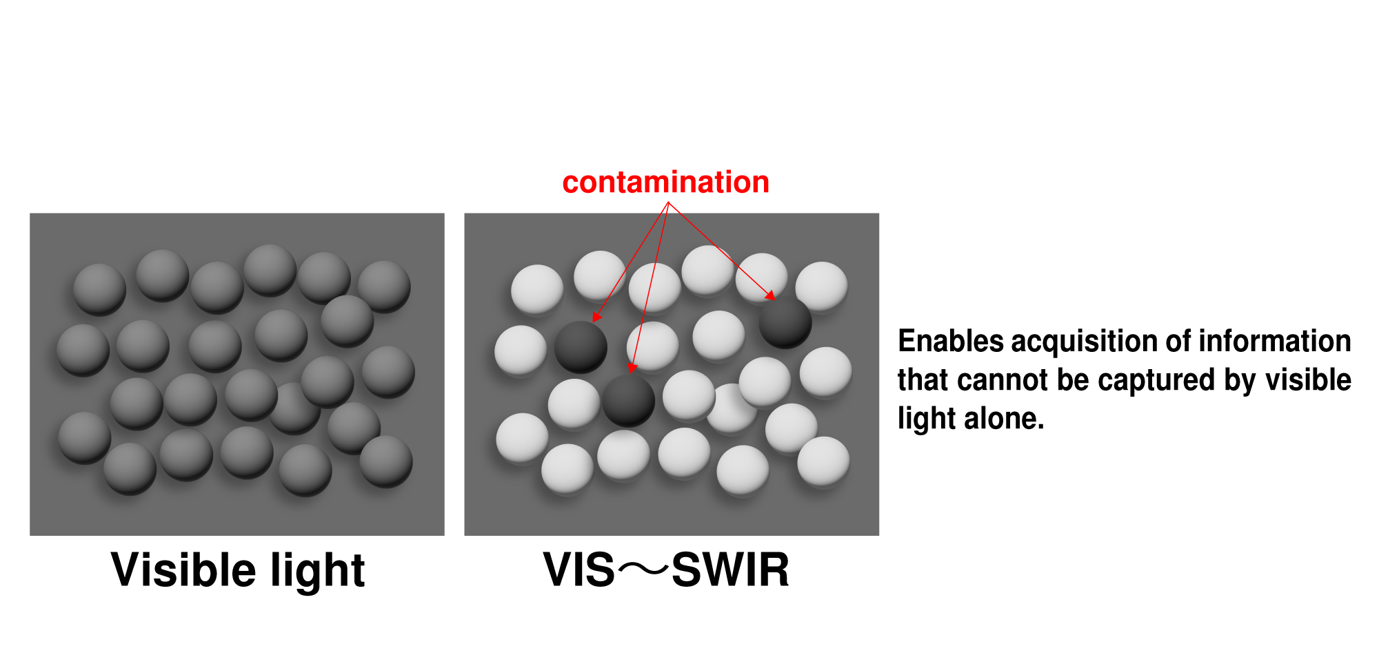
Figure 2: Image of Contamination Detection (left: VIS only; right: from VIS to SWIR)
<The Semiconductor Laboratory, College of Engineering, Ibaraki University (in charge: Prof. Haruhiko Udono)>
- The Semiconductor Laboratory conducts research and development of optical, electronic, and thermal functional elements utilizing silicide semiconductors. The laboratory is particularly focused on research into infrared sensors, thermal photovoltaic cells, and thermoelectric conversion elements that convert light and heat energy into electrical energy, from basic to practical applications. Please click here to visit the Semiconductor Laboratory website.