Products Under Development
Under DevelopmentMg2Si Single Crystal for Infrared Detector
Joint research between Ibaraki University and JX Nippon Mining & Metals
Mg2Si (Magnesium Silicide) single crystal is a semiconductor material that can detect a wide range of wavelengths, from visible light (VIS) to near infrared (NIR) and shortwave infrared (SWIR), and is expected to be used for various sensors.
Application Examples
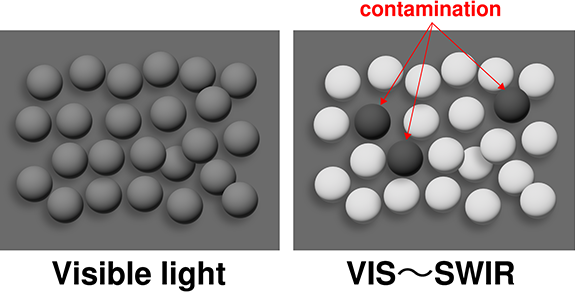
Enables acquisition of information that cannot be captured by visible light alone.
Image of contamination inspection
Application Examples for Mg2Si Single Crystal
- Image Sensors
- Contamination inspection
- Crop inner-damage evaluation
- Surveillance cameras unaffected by fog
- 3D Sensing
- LiDAR
- Others
- Blood glucose sensor
- Water content measurement
etc.
What Can Be achieved with Mg2Si Single Crystal
- Detects a wide range of wavelengths from visible light (VIS) to near infrared (NIR) and shortwave infrared (SWIR) with Mg2Si single material.
- High crystallinity enables fabrication of high-sensitivity photodiodes. (Rocking curve: FWHM = 8 arcsec)
- Since photo-detection function can be achieved using Mg2Si alone, a simple device structure consisting of a PN-junction of the Mg2Si layer can be used. (no hetero-epitaxial growth required)
- Carrier concentration (1016–1019 cm-3) and P/N conduction type can be easily controlled by impurity doping.
- Non-toxic and RoHS compliant.
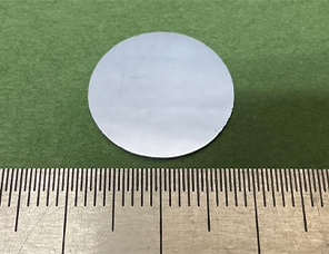
- Bulk single-crystal wafers of 2 inches and larger are under development.
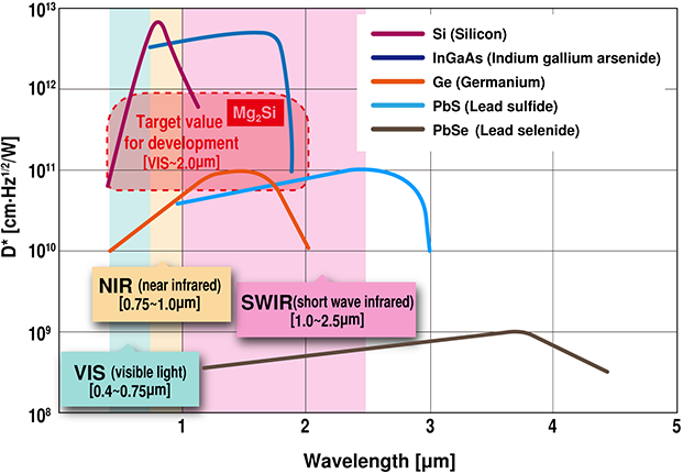
Detection Wavelength Range of Mg2Si
- Detects a wide range of wavelengths from visible light (VIS) to near infrared (NIR) and shortwave infrared (SWIR) with a single material.
- Mg2Si can detect a wider range of wavelengths than Si, into the infrared range.
- Mg2Si is expected to have higher detection sensitivity (D*) than Ge.
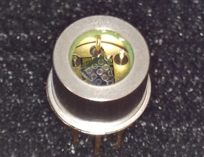
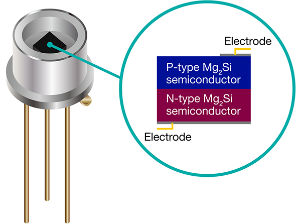
Example of Device Structure Using Mg2Si
- Since the photo-detection function can be achieved using Mg2Si alone, a simple device structure consisting of a PN-junction of the Mg2Si layer can be used (no hetero-epitaxial growth required).
- Mg2Si single crystal can be used in the bulk region as a photo absorber, whereas InGaAs and other materials require hetero-epitaxial growth on substrates to form thin films as photo absorbers.
Contact Information
From the Web
Inquiries accepted 24 hours a day