News Release
FY2023
July 26, 2023
Joint Research with AIST Speeds Up Social Implementation of Printed Electronics
JX Metals Corporation (President: Hayashi Yoichi; "the Company") is conducting joint research1 with the National Institute of Advanced Industrial Science and Technology (President and CEO: Ishimura Kazuhiko; "AIST") to develop fine wiring formation technologies for next-generation devices using printed electronics (PE). Having recently succeeded in using screen offset printing2 to form fine copper wiring with a line width of 6 μm, the highest level of fineness in the world, the Company has decided to launch full-scale marketing activities aimed at social implementation, starting with a reference display at a trade fair.3
PE is a technology that forms wiring by printing ink infused with conductive materials onto resin films and glass substrates. PE is said to enable formation of even finer wiring than the conventional copper foil etching method and is expected to contribute to further miniaturization and thinning of smartphones and wearable devices. Moreover, it is predicted to simplify manufacturing processes compared to the conventional etching method. Since wiring is formed by printing only the necessary amount, PE can also help reduce energy and materials consumption. The joint research project has been able to form fine copper wiring by merging copper ink materials technology using the Company's fine copper powder with AIST's printing technology. As well as pursuing even finer wiring, establishing mass production technologies, and optimizing processes, the Company will gather information on market needs through dialogue with customers at trade fairs, etc. and explore various applications.
The JX Metals Group will continue to actively engage in product development through co-creation with partners, unite in steadily implementing its growth strategy, and contribute to innovation and the development of a sustainable society as a global leader in advanced materials.
Reference materials
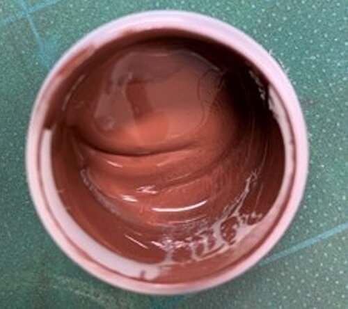
Copper ink produced by the Company
Our achievement example of joint research (Fine copper wiring formed on resin film)
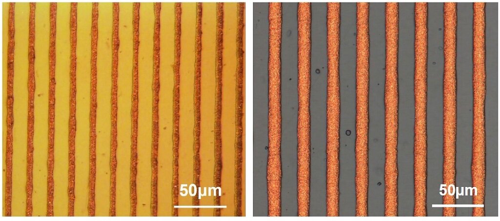
L/S = 6/14 μm L/S = 15/15 μm
Note: L/S is an abbreviation of "line and space," denoting circuit wire width and gap between circuits.
Source: Y. Kasashima et al., Jpn. J. Appl. Phys. 61, SE1001 (2022)
- For details of joint research between the Company and AIST, see news release dated November 1, 2021,
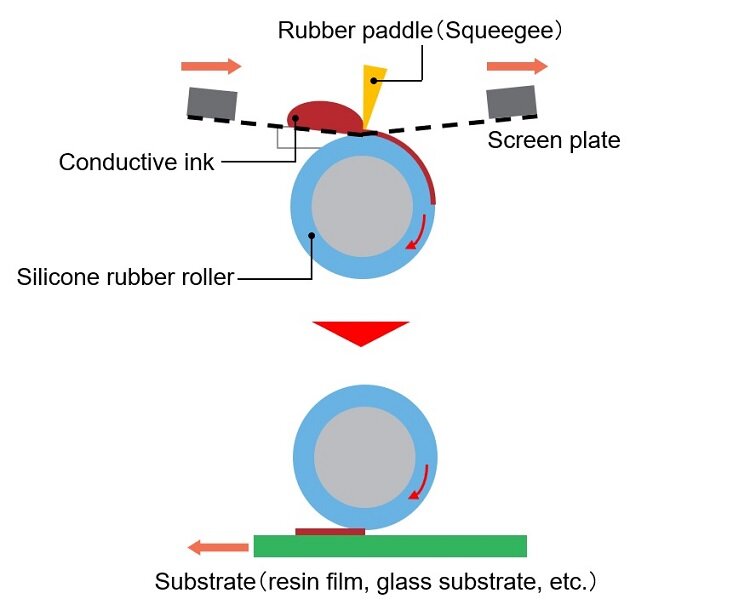
"Establishment of JX Metals-AIST Advanced Material and Technology for Future Society Cooperative Research Laboratory" - Screen offset printing is a method of screen-printing conductive ink onto a silicone rubber roller for transference, and then transferring the conductive ink printed on the roller to a substrate to form a pattern. The convenient process makes it simple to printed large areas and enables high printing speeds. Since the roller absorbs solvents in the conductive ink, it is possible to control ink bleeding and print fine wiring.
Source: K. Nomura et al., Microelectron. Eng. 197, 23 (2018), etc.