News Release
FY2023
June 30, 2023
JX Metals Corporation
JX Metals and Gaianixx Begin Collaboration for Social Implementation of Innovative Semiconductor Formation Technology
--Partnership with Startup Launched by The University of Tokyo Aims for New Developments in Crystal Materials Business--
JX Metals Corporation (President: Hayashi Yoichi; "the Company") has acquired shares to the value of 300 million yen in Gaianixx Inc. (Chief Executive Officer: Nakao Kento; "Gaianixx") through a third-party allocation of newly-issued shares.
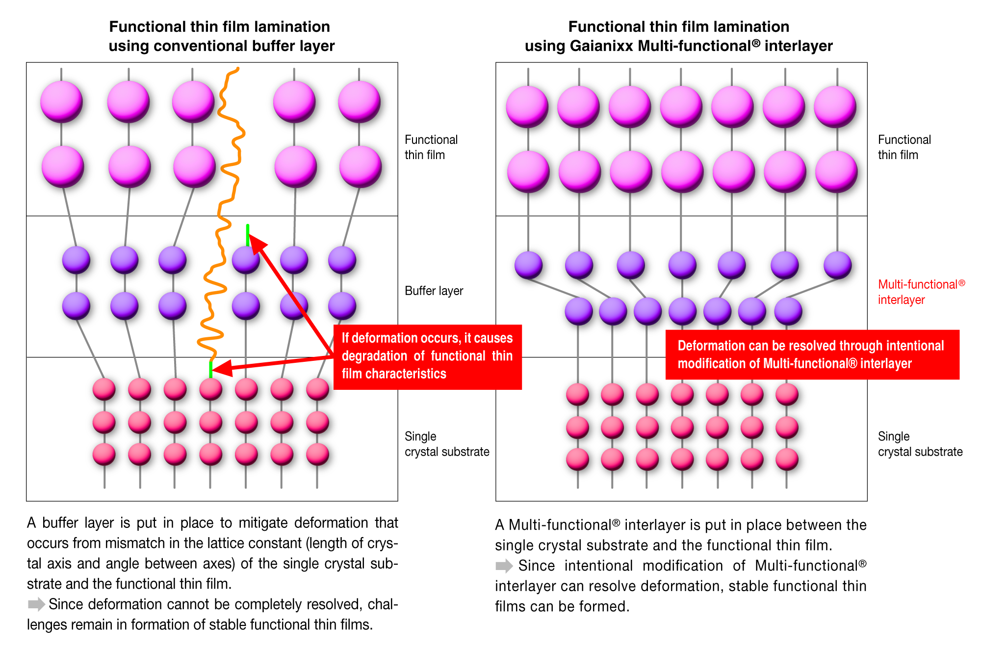
Hopes are currently high for the emergence and widespread use of innovative devices that will drive progress in the data society and decarbonization. Advances in semiconductor devices are essential to such progress. These include piezoelectric elements that support sensing technologies and advanced communications as well as power semiconductors enabling innovation in power supply systems for applications such as electric vehicles. Crystal materials forming functional thin films1 on single-crystal substrates are used in such semiconductor devices, and resolving deformation that occurs between single-crystal substrates and functional thin films is a challenge for further improving the performance and added value of semiconductor devices.
Gaianixx aims to use its original Multi-functional® interlayer technology to resolve this challenge.2 Since Multi-functional® interlayer technology can resolve deformation through repeated modification regardless of the combination of single crystal substrate and functional thin film materials used, it enables lamination of higher-quality functional thin films. This is a breakthrough in semiconductor device formation, and practical application of this technology will spur innovative advances in semiconductor element performance, reliability, and yield.
This investment in Gaianixx creates opportunities for conducting joint development of materials such as sputtering targets and high-purity metals used in Multi-functional® interlayer as well as functional thin films. Moreover, the Company will utilize its extensive worldwide networks in the semiconductor industry to promote industry-based commercialization of the innovative technologies and products that Gaianixx possesses. These efforts will lead to new developments in crystal materials business, which the Company is expanding in scale.
The Company will continue to proactively develop products and technologies through co-creation with its partners, and contribute to the creation of a sustainable society by proposing and supplying cutting-edge materials essential to innovative electronic devices.
1. Various methods are used to form functional thin films, but recent R&D has focused on lamination using the sputtering method. Details on the sputtering method are available here.
2. The diagrams below show differences between regular crystal materials and those used in Gaianixx technology.
For reference: Overview of Gaianixx Inc. (as of May 31, 2023)
| Company name | Gaianixx Inc. |
| Establishment | November 2021 |
| Location | Entrepreneur Labo, South Clinical Research Building, the University of Tokyo |
| Capital | 100,000,000 yen |
| Business activities | Research and development of Multi-functional® interlayer and epitaxial growth technologies as well as manufacture and sale of products using these technologies. |
| Website | https://gaianixx.com/ |